Tel: 136-0396-0595
Email: lyxcxcl@163.com
Address: Baiying Village, Xindian Town, High tech Zone, Luoyang City
Key characteristics
Ultra thin thickness:
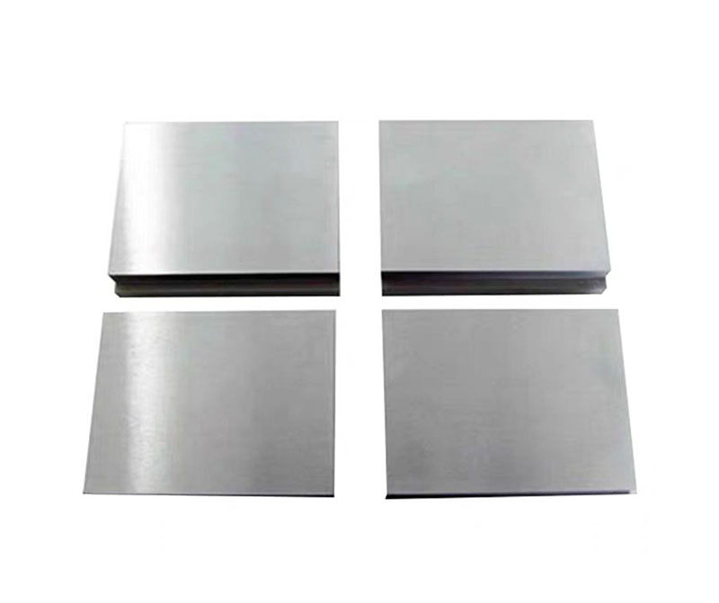
Molybdenum foil:thickness≤0.1mm(commonly 0.01~0.1mm),can be as low as 5μm(special process required).
Molybdenum sheet:thickness of 0.1-1mm,balancing strength and plasticity.
High purity:≥99.95%(3N5)or higher(such as 99.99%),with minimal impurities,to avoid high-temperature grain boundary embrittlement.
Surface accuracy:requires polishing or electrolytic treatment,with a roughness Ra≤0.2μm(for electronic devices).
Flexible processing:Ultra thin molybdenum foil can be bent or stamped into complex shapes(but repeated bending should be avoided to prevent breakage).
Core applications
Molybdenum foil(ultra-thin)
Electronic packaging:a heat dissipation substrate for power semiconductors(such as IGBT).
Flexible display:OLED vapor deposition mask plate(replacing traditional Invar alloy).
Nuclear industry:isotope separation membranes,radiation shielding layers.
Research field:Synchrotron radiation light source window materials(high transmittance and radiation resistance).
Molybdenum sheet(slightly thick)
Vacuum electronic devices:traveling wave tube,magnetron electrode.
High temperature sensor:thermocouple protective cover,lining of high temperature reaction vessel.
Photovoltaic backsheet:a flexible substrate for thin-film solar cells(requiring copper or aluminum plating on the surface).
Production process
Rolling technology:
Multi pass cold rolling(more than 20 passes required for thickness<0.1mm),intermediate annealing(in a hydrogen environment at 1200℃)to eliminate work hardening.
The foil material requires a foil rolling mill(such as a Sendzimir rolling mill)to control the tension and prevent breakage of the strip.
Surface treatment:
Electrolytic polishing:reduces microcracks and improves surface smoothness.
Plasma cleaning:Removing residual organic matter(used in semiconductor processes).
Cutting process:laser cutting or precision etching(to avoid warping caused by mechanical stress).

Hotline
136-0396-0595
Enterprise WeChat

Mobile Station
BACK TO TOP
 136-0396-0595